Our semiconductor wafer sort solutions combine precise automated wafer probing with advanced engineering to ensure high accuracy, repeatability, and throughput.
This section provides a closer look at our probe card technologies and wafer sort capabilities that are designed to meet the specific electrical and mechanical requirements of each device while enabling early defect detection and yield optimization.


Equipped with fully automated wafer probers integrated into advanced ATE test cells, enabling high-throughput and precision wafer-level testing for logic, mixed-signal, and RF devices across 8” and 12” wafers, including sawn wafer probing.


Our advanced wafer probing processes integrate embedded risk safeguards and stringent manufacturing quality controls.


Equipped with multiple docking solutions—including direct dock, standard hard dock, and cable/soft dock configurations—enabling full compatibility and mechanical/electrical interface support across a wide range of ATE platforms such as Teradyne, Advantest, and Cohu.


High parallelism of up to 32 sites for WLCSP and 1280 for Pad wafers.
Temperature range
-55˚C to +150˚C

Frame probing on Singulated and Fan-Out wafer.

Blackbox testing
Security Key Encryption on wafer level.

Wafer size
8″ and 12″

Software customization
support GDBN and PAT* to drive toward zero defect.

Strategic partnership
long term partnership with foundries and probe card suppliers.

In-house support
Certified In house Probe card maintenance team.
Multiple Probe Card Technologies

Up to 16 Sites
1752 Pin Counts
40um x 40um Pad Size
Bump Pitch 200/400um
Up to 16 Sites
1052 Pin Counts
40um x 40um Pad Size
Bump Pitch 200/400um

Up to 1280 Sites
Pin Counts 26000
Pad Size 55um
Bump Diameter 85um
Bump Pitch 64um/880um

Up to 192 Sites
Pin Counts 1764
Bump Diameter 80um
Bump Pitch 150um

Up to 8 Sites
Pin Counts 1762
Bump Diameter 85um
Bump Pitch 200/400um

Up to 1226 Sites
Pin Counts 4912
Pad Size 50um x 60um
Pad Pitch 60um

Extensive hands-on experience with a wide range of probe card technologies, including vertical, cantilever, MEMS, and advanced fine-pitch probe cards, supporting various wafer-level test applications across logic, memory, mixed-signal and RF devices.
| Highest Parallelism | 8 Sites |
| Maximum Pin Count | 1762 Pins |
| Bump Diameter | 85 um |
| Bump Pitch | 200 um / 400 um |
| Highest Parallelism | 1226 Sites |
| Maximum Pin Count | 4912 Pins |
| Smallest Pad Size | 50um x 60um |
| Minimum Pad Pitch | 60 um |
| Highest Parallelism | 16 Sites |
| Maximum Pin Count | 1752 Pins |
| Smallest Pad Size | 40um x 40um |
| Closest Bump Pitch | 200um / 400um |
| Highest Parallelism | 1280 Sites |
| Maximum Pin Count | 26000 Pins |
| Smallest Pad Size | 55um x 55um |
| Bump Diameter | 85um |
| Bump Pitch | x = 64um, y = 80um |
| Highest Parallelism | 32 Sites |
| Maximum Pin Count | 1764 Pins |
| Bump Diameter | 80um |
| Bump Pitch | 150um |

Comprehensive probe card management services supported by deep engineering expertise, encompassing the full lifecycle— from design review and technology selection to maintenance, performance monitoring, and failure analysis—ensuring optimal electrical performance, mechanical integrity, and test yield.

High Magnification Scope, measuring pin tip length, tip diameter, useable tip. Magnified view of the dirt, FM.

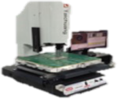
PB Analyzer (PB3600).
Tweaking to adjust alignment. Push and pull to adjust planarity.

First Level
In-house support

Physical Hardware
Storage Rack

Probe card Management Database
Ready to leverage our highly comprehensive, high-volume IC testing ATE infrastructure? Our 2,000+ test platforms are configured and waiting to accelerate your semiconductor testing requirements.