Background Image
Background

Laminate Substrate Technology: Maximizing Semiconductor Capabilities

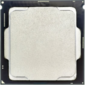
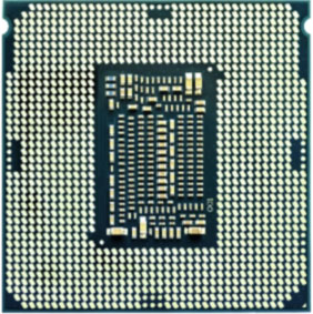
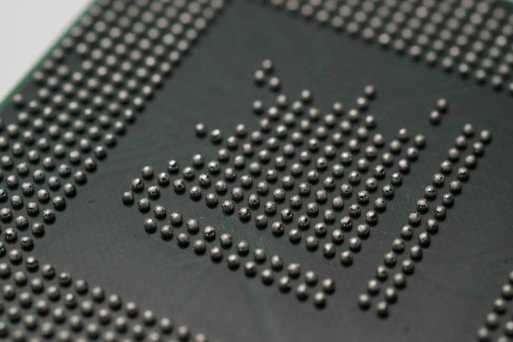
A laminate substrate is a type of material used as a base or platform for semiconductor packages. It serves as the structural foundation for connecting a semiconductor chip to the external circuitry. These package substrates are typically made of layers of reinforced resin materials (such as epoxy) combined with copper foils, forming a multilayer structure.

Key Features of Laminate Substrates

Material Composition:

Material Composition::

The core material is often a resin (e.g., epoxy) reinforced with materials like glass fiber for strength and thermal stability.

Copper layers are used to create electrical pathways and interconnections.

Structure:

Structure::

They are multilayered to accommodate complex interconnections and routing for high-performance chips.

Inner layers provide electrical pathways, while the outermost layers often include solder mask coatings to protect the circuitry.

Thermal and Electrical Properties:

Thermal and Electrical Properties::

Designed to handle thermal management needs and ensure proper electrical conductivity.

Dielectric layers provide insulation between conductive layers.

How Laminate Substrates Are Used

Chip Attachment

Chip Attachment

  • The semiconductor die (chip) is mounted on the laminate substrate using bonding materials like solder or adhesives.
  • The electrical connections between the chip and the substrate are established via wire bonding, flip-chip bonding, or other methods.
Interconnections

Interconnections

  • The laminate substrate routes electrical signals from the chip to external leads or pads that connect to a printed circuit board (PCB).
  • This routing is achieved through copper traces embedded in the substrate.
Packaging

Packaging

  • The substrate is encapsulated along with the chip in a protective material (like epoxy resin) to form the final semiconductor package, such as a ball grid array (BGA) or chip-scale package (CSP).
Thermal Management

Thermal Management

  • The substrate helps dissipate heat generated by the semiconductor during operation, often incorporating thermal vias or conductive planes to enhance heat transfer.
Applications

Applications

Laminate substrates are widely used in various semiconductor package types, including:

Background
Ball Grid Arrays (BGAs)
Chip-Scale Packages (CSPs)

Advantages

  • Cost-effective compared to ceramic substrates.
  • Scalable for high-volume production.
  • Supports high-density interconnects for advanced chips.

Challenges

  • Thermal and mechanical limitations compared to ceramics, making them less suitable for extreme environments.

In summary, laminate substrates are crucial components in semiconductor packaging materials, providing a robust platform for chip attachment, electrical routing, and thermal management, enabling the integration of chips into electronic systems.

Image Image

Partner with UTAC for Industrial electronics semiconductor testing and packaging solutions.

Contact us today to explore how our industrial automation solutions can maximize your performance and operational efficiency.

Enquire Now