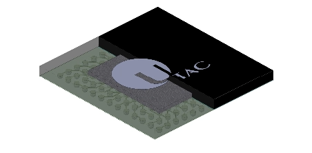
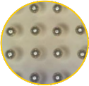
Wafer-Level Chip Scale Packaging (WLCSP) offers compact, cost-effective solutions that enhance performance and thermal efficiency. Combined with precision bumping technology, our WLCSP solutions ensure reliable electrical connections and meet the needs of high-density applications in mobile, automotive, and computing sectors.
Package Structure:
0P1M / 1P1M / 2P2M
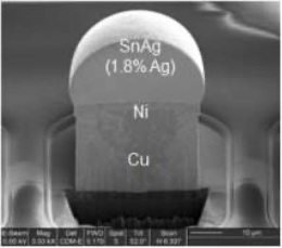
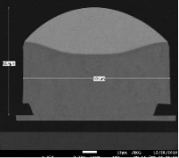
Bump Structure:
Cu/Ni/SnAg or Cu/SnAg with RDL option
Passivation:
Low temp / High temp PI & PBO including PFAS-free & low stress options
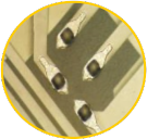
Package Structure:
1P1M / 2P2M
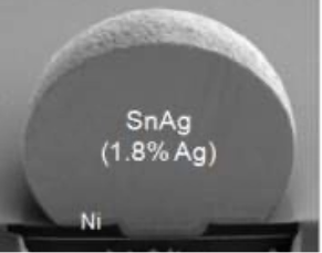
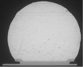
Bump Structure:
Ni/SnAg with RDL option
Passivation:
Low temp / High temp PI including PFAS-free & low stress options
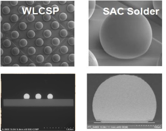
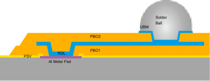
Package Structure:
1P1M / 2P2M / 3P3M (dev) + Ball Mount
RDL & UBM:
Thick RDL & UBM options available
Solder Ball:
SAC405 / SACQ / LF35
Ball Pitch:
300 – 500um
Passivation:
Low temp / High temp PI & PBO including PFAS-free, low stress and thick PBO options


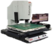
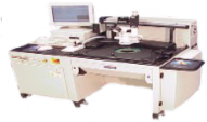
High Parallelism
Up to 32 sites for WLCSP and 1280 for Pad wafers

Temperature Range
-55˚C to +150˚C

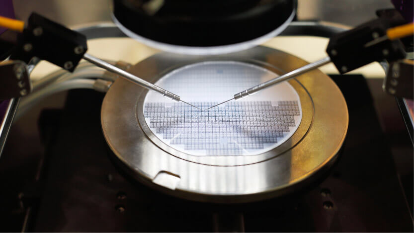
Frame Probing
Singulated and Fan-Out Wafer

Blackbox Testing
Security Key Encryption on Wafer Level

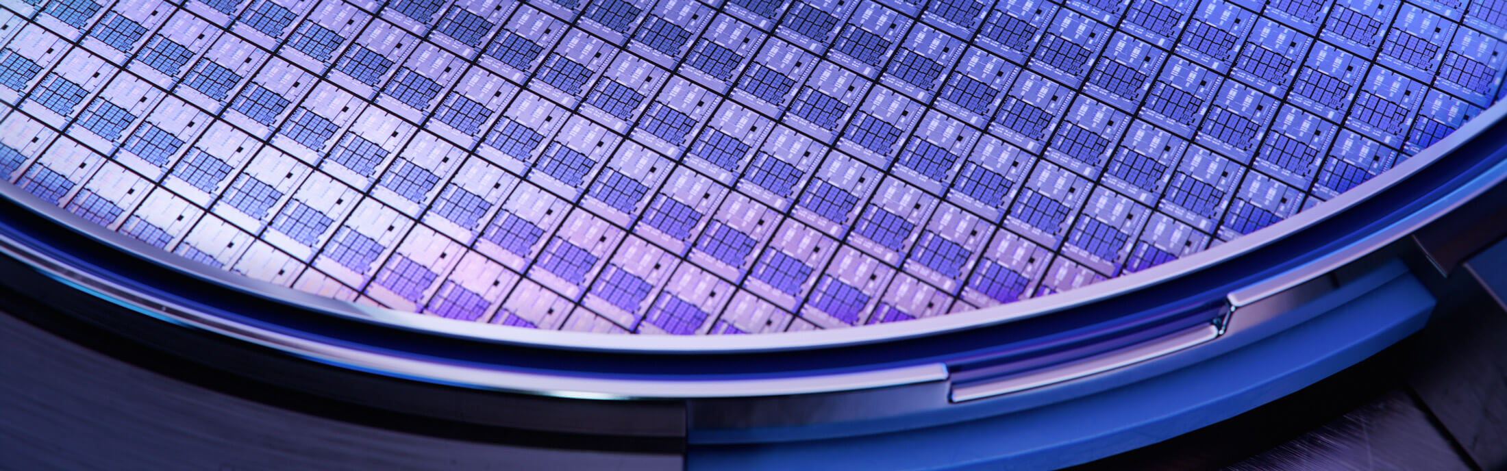
Wafer Size
8″ and 12″

Software Customization
Support GDBN and PAT* to drive toward zero defect”

Strategic Partnership
Long term partnership with foundries and probe card suppliers.
Multiple Probe card Technologies

Certified In house Probe card maintenance team.
Multiple Probe card Technologies