Background Image
Image

Engineering Flip-Chip Chip-Scale Packaging Excellence

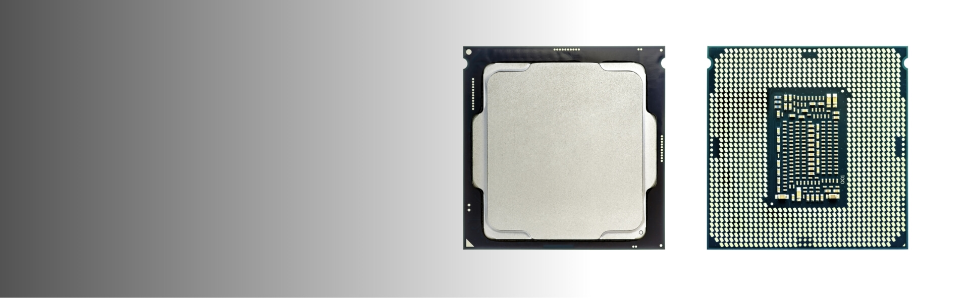
FCCSP stands for Flip-Chip Chip-Scale Package. It is a type of semiconductor packaging technology that combines flip-chip bonding with the benefits of a chip-scale package (CSP).

FCCSP is widely used in applications requiring compact, high-performance, and high-density packaging, such as in mobile devices, consumer electronics, and high-speed computing.

Key Features of FCCSP Packaging

Explore the advanced technical features that make flip chip integration an optimal choice for high-performance applications.

Flip-Chip Bonding
Flip-Chip Bonding
  • The semiconductor die is flipped upside down so that its active surface (where the input/output (I/O) pads are located) faces the substrate.
  • Tiny solder bumps on the die make direct electrical connections to the substrate, eliminating the need for wire bonding.
Chip-Scale Package (CSP)
  • CSP refers to packages that are nearly the same size as the chip itself, offering a compact and lightweight design.
  • FCCSP achieves a small form factor ideal for space-constrained devices.
Multilayer Substrate
  • Typically, a laminate substrate is used in Flip Chip CSP (FCCSP), providing electrical routing and mechanical support.
  • The substrate often includes multiple layers to handle high I/O density and complex signal routing.
Encapsulation
Encapsulation
  • After assembly, the chip and substrate are encapsulated to protect the solder joints and chip from mechanical and environmental stresses.
Ball Grid Array (BGA) Interface
  • The package uses an array of solder balls on the bottom of the substrate to connect to the printed circuit board (PCB).
Background

How FCCSP is Used

Whether you’re developing solutions for automotive, mobile, computing, or industrial applications, our experienced team will work closely with you to optimize your package design and manufacturing process.

How FCCSP is Used
Assembly Process

Assembly Process

  • The flip-chip die is placed on the substrate, and the solder bumps are reflowed to establish electrical and mechanical connections.
  • Underfill material is added between the die and substrate to enhance mechanical reliability and thermal stability.
Electrical Interconnections

Electrical Interconnections

  • Electrical signals are routed through the solder bumps to the substrate, then through the substrate to the BGA, which interfaces with the PCB.
Thermal Management

Thermal Management

  • FCCSP allows for better heat dissipation compared to traditional wire-bond packages because the flipped die ensures shorter electrical paths and closer contact to the substrate.
Integration with PCBs

Integration with PCBs

  • The BGA balls on the substrate’s bottom are soldered to corresponding pads on the PCB, forming the final connection in an electronic system.

FCCSP Applications for Maximum Miniaturization

FCCSP is commonly used in:

Mobile devices
Mobile devices

Smartphones and tablets, where size and performance are critical.

Consumer electronics

Cameras, gaming consoles, and wearable devices.

Automotive electronics

Advanced driver-assistance systems (ADAS) and infotainment systems.

High-performance computing

Processors, GPUs, and memory modules.

Advantages of FCCSP Packaging

Advantages of FCCSP Packaging

FCCSP offers significant advantages over conventional packaging solutions, including:

Compact size
Compact size

Ideal for small, lightweight designs.

High performance
High performance

Shorter interconnections improve electrical performance.

Efficient heat dissipation

Flip-chip design enhances thermal management.

High density
High density

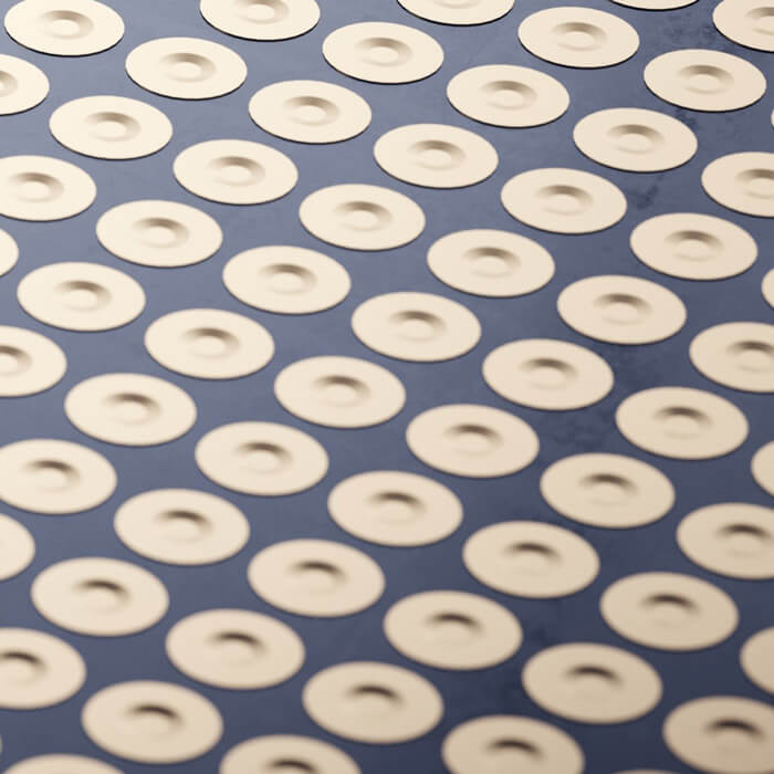
Accommodates high I/O counts in a small area.

Challenges of FCCSP Packaging

Below are the technical considerations required to successfully implement FCCSP solutions:

Cost
Cost
Flip chip assembly and substrate materials are more expensive than traditional packaging.
Complexity
Complexity
Requires precise manufacturing and handling.
Reliability
Reliability
Solder bump and underfill quality are critical to long-term performance.
Background

Flip-Chip Chip-Scale Packaging (FCCSP) has become a critical packaging technology for modern electronics, balancing size, performance, and functionality to meet the demands of advanced applications.

Image Image

The UTAC Edge For FCCSP Technology Expertise

As a trusted partner to leading semiconductor companies worldwide, UTAC Group delivers superior quality, reliability, and performance.

Contact our team today to discover how to power your next-generation devices with UTAC Group’s comprehensive FCCSP packaging and testing services.

Schedule a consultation with our packaging specialists