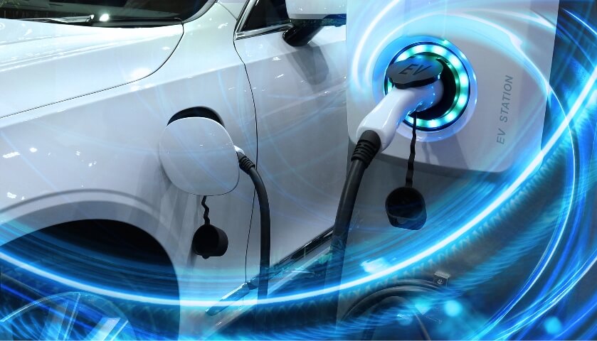
In a world increasingly reliant on wireless communication devices and mobile connectivity solutions, from smartphones to networking infrastructure, semiconductor solutions are driving the technology behind a wide range of applications.

As demand for faster, more reliable, and secure communication grows, the semiconductor industry is continuously innovating with advancements across wired and wireless communication devices, optical, network infrastructure, mobile connectivity solutions, IoT and 5G applications and satellite communications.
UTAC Group is highly active in the communications IC market, providing advanced semiconductor packaging for smartphones and infrastructure applications.
Our expertise in high-frequency packaging solutions spans the entire communications ecosystem of consumer devices and infrastructure applications.


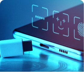

We leverage our long-standing expertise in wafer sort and wafer level packaging to address many smartphone applications for major smartphone OEMs:
For power and RF applications requiring excellent thermal dissipation and low-loss, high frequency operation.
For high frequency applications due to their lower parasitic inductance and capacitance.
For highly integrated modules and sensor applications.


From bumping, wafer sorting, assembly and final test.
We can offer the entire flow for wafer level packaging in a location renowned for its high engineering expertise, geopolitical stability and supply chain resilience.
Our expertise and quality standards meet the stringent performance and quality criteria required for devices destined for flagship smartphones.